TDI Cameras: Sharper, Faster, Brighter
Table of Contents
TDI cameras (Time Delay and Integration Cameras) are a new type of line scan camera featuring an area array structure but line array output. Leveraging technical advantages such as high-speed scanning, large area coverage, and high-resolution imaging, TDI cameras have become core components in high-end inspection equipment.
What Are TDI Cameras?
TDI cameras (Time Delay Integration Cameras) are high-performance line scan cameras specifically designed for imaging objects moving at high speed. Through a unique charge synchronous transfer mechanism, they can obtain high-resolution, clear images even under extremely low light conditions.
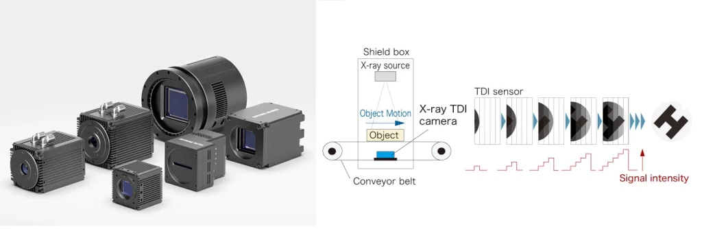
TDI cameras are suitable for applications where one wishes to record linear processes over time, or where the aspect ratio of the object is significantly asymmetric. They are especially useful for scanning applications under low-light conditions, where ordinary line cameras fail to produce usable images.
Principle and Operation of TDI Cameras
Principle of TDI Cameras
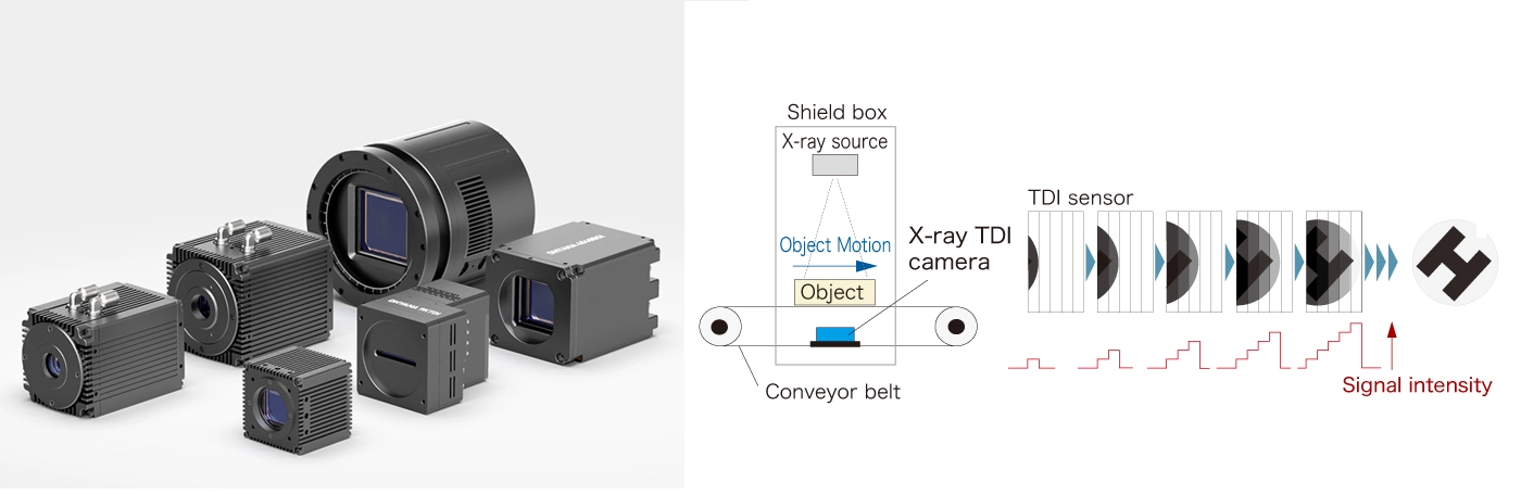
–Synchronous Dynamic Acquisition Mechanism: As the sample moves continuously at a constant speed, TDI sensors achieve precise synchronization between pixel columns and the motion speed, enabling continuous exposure and dynamic charge accumulation on the same target. This “exposure on the move” mode compensates for blur and distortion caused by the motion of the target or the camera itself, resulting in clearer and more detailed images.
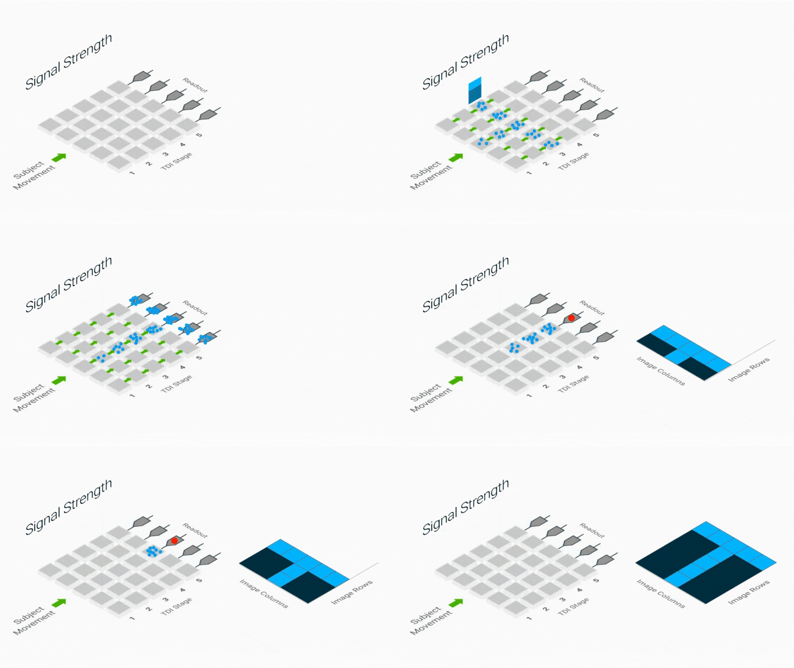
–Multi‑Stage Charge Accumulation Gain: Each column of pixels converts received light signals into charges, which are then accumulated through multi‑stage shift registers – equivalent to superimposing and amplifying the weak signal N times. Under the same luminous flux conditions, this significantly improves imaging quality in low‑light environments, thereby reducing system power consumption and cost. Moreover, in push‑broom imaging, it can largely eliminate image motion blur.
The principle can be described by the following mathematical model:
S(x) = Σ(i=1 to N) Pi(x)
Where:
S(x) = final output signal; N = number of TDI stages (i.e., number of pixel rows)
Pi(x) = light signal received by row i at position x
This formula clearly expresses the core idea of TDI technology: enhancing signal strength through multiple accumulations.
Operation of TDI Cameras
When light strikes the first row of pixels, an initial photocharge is generated.
—In the next clock cycle, this charge is precisely transferred to the second row of pixels.
—Meanwhile, the first row continues to receive new photons and generate new charges.
—This process continues through subsequent rows – each row receives new photons and accumulates charges from the previous row.
—When the charge reaches the last row, the accumulated signal is read out, forming the final image signal.
Advantages of TDI Cameras
Compared with traditional line scan cameras, TDI cameras offer the following advantages:
–Higher Sensitivity: Through global shutter and high-speed signal processing circuitry, TDI cameras can freeze high-speed moving objects with microsecond precision. For example, in semiconductor inspection, they can capture wafer defects moving at several meters per second. Because signals can be accumulated across multiple pixels, TDI cameras can capture more photons within the same exposure time, thereby improving sensitivity.
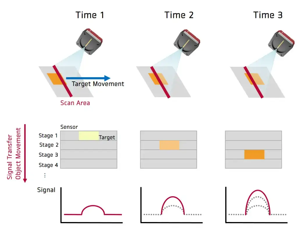
The sensitivity improvement can be quantified by:
Sensitivity improvement = N × Single‑line sensitivity (where N is the number of TDI stages)
–Higher Dynamic Range: TDI technology allows more photons to be captured without saturation, thereby expanding the camera’s dynamic range. The dynamic range improvement can be estimated by:
Dynamic range improvement ≈ log₂(N) + Single‑line dynamic range
This means that, for example, 128‑stage TDI can theoretically add about 7 bits of dynamic range.
–Higher Line Rate: Because each pixel receives light for a longer period, TDI cameras can operate at higher line rates while maintaining good image quality. The latest TDI cameras have achieved astonishing line rates up to 5000 kHz, unimaginable for traditional line scan cameras.
Recommended In-depth Reading from AI Robots Eidos
To avoid misleading readers, AI Robots Eidos points out that traditional line scan cameras and TDI cameras each have their own characteristics. Traditional line scan cameras also have their advantages: simpler structure (mostly one row or a few rows), lower manufacturing and production costs, and simpler system integration and debugging – no need for precise synchronization of multi‑row charge transfer as required by TDI cameras.
If you wish to better understand line scan cameras, please read this detailed article on line scan cameras.
Challenges and Solutions for TDI Cameras
Despite their many advantages, TDI cameras face several technical challenges:
–Precise Synchronization: TDI technology requires that the charge transfer speed exactly matches the object motion speed. In practice, achieving absolute synchronization is difficult; even minor mismatches can cause significant image degradation. To address this, modern TDI systems typically employ sophisticated feedback control systems and adaptive algorithms
–Dark Current Accumulation: Because charges are accumulated across multiple pixels, dark current also accumulates, potentially increasing noise. The variation of dark current I_dark with temperature T and TDI stage number N can be described by the simplified model:
I_dark ≈ N × I₀ × exp(-Eg/(2kT))
Where:
I₀ = material‑dependent constant; Eg = semiconductor bandgap energy
k = Boltzmann constant
To reduce the impact of dark current, techniques such as sensor cooling and dark current compensation algorithms are typically used.
–Charge Transfer Efficiency: During multiple charge transfers, charge loss may occur. Charge Transfer Efficiency (CTE) is an important parameter measuring this process. For N‑stage TDI, the total CTE is:
CTE_total = (CTE_single)^N
Where CTE_single is the single‑transfer efficiency. This shows that even if single‑transfer efficiency is high, the cumulative effect after many transfers can be significant. To maintain high image quality, modern TDI sensors typically require CTE_single ≥ 0.99999.
TDI Camera Product Parameters (For Reference Only)
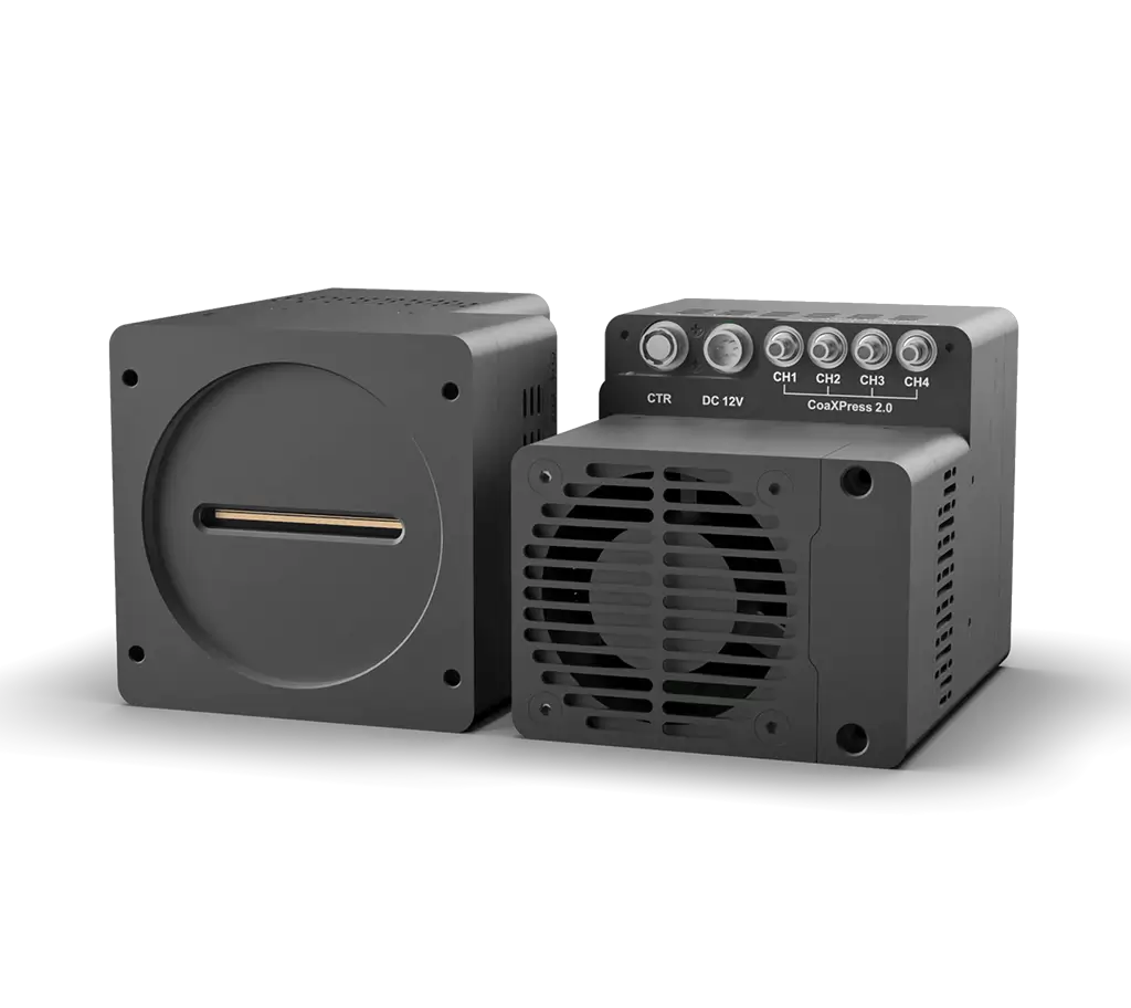
| Parameter | Value |
| Sensor Type | Back-illuminated CMOS |
| Sensor Model | GLT5009BSI |
| Resolution | 9072 (H) x 256 (V) |
| Monochrome/Color | Monochrome |
| Active Area Size | 45.36mm x 1.28mm |
| Pixel Size | 5μm x 5μm |
| Quantum Efficiency | 82%@550nm, 50%@350nm, 38%@800nm |
| TDI Stages | 4, 8, 16, 32, 64, 96, 128, 160, 192, 224, 240, 248, 252, 256 |
| Scanning Direction | Bidirectional |
| Charge Transfer Efficiency | ≥0.99993 |
| Data Bit Depth | 12bit, 10bit, 8bit |
| Full Well Capacity | 16ke-@12bit; 14ke-@10bit |
| Dynamic Range | 69 dB |
| Maximum Line Rate | 300kHz@12bit; 350kHz@10bit; 510kHz@8bit |
| Dark Signal Non-Uniformity | 1e- |
| Photo Response Non-Uniformity | 0.30% |
| Cooling Method | Air-cooling & Water-cooling |
| Maximum Cooling Temperature | 40°C below the water temperature |
| Pixel Binning | 2×1; 4×1; 8×1 |
| Timestamp Accuracy | 8 ns |
| Gain | Analog: x2 ~ x8; Digital: x0.5 ~ x10 |
| Trigger Input | Trigger Input, Scan Direction Input |
| Trigger Output | Strobe out |
| External Trigger Interface | Horison |
| Data Interface | CoaxPress 2.0 |
| Optical Interface | M72, customizable |
| Power Supply | 12V/8A, HR-10A-6P-PB connector |
| Power Consumption | <60W |
| Camera Dimensions | 86mm x 86mm x 109mm |
| Camera Weight | 1100g |
| Application Software | Samplepro/Matlab |
| SDK | GenICam standard support |
| Compatible OS | Windows/Linux |
Specific Applications of TDI Cameras
–Aerospace and Remote Sensing: By superimposing multiple images to enhance brightness, TDI cameras can obtain clear images even under low‑light conditions. Leveraging this advantage, TDI cameras can be mounted on satellites to capture clear topographic images in Earth’s shadow regions or low‑light environments for geographic mapping, environmental monitoring, and resource exploration. They can also be used for deep‑space exploration due to their ability to detect extremely weak light signals.
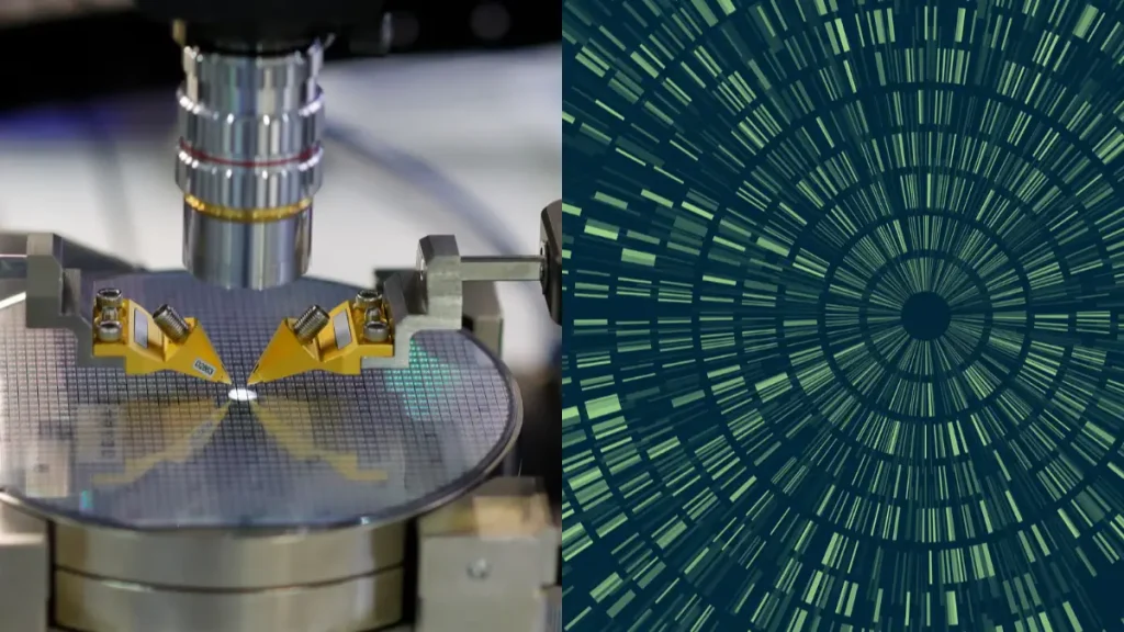
–Semiconductor Industry: Utilizing features such as high resolution (up to 16k pixels/line), high sensitivity (down to single‑photon level), high line rates (now up to 5000 kHz), and dynamic range exceeding 90 dB, TDI cameras excel in semiconductor wafer inspection. They can detect defects at the sub‑micron level while meeting the high‑speed scanning requirements of large‑format (12‑inch) wafers. As IC manufacturing moves toward 5nm processes, inspection system demands continue to rise. With deep integration of AI and machine learning algorithms, TDI cameras are expected to enable more intelligent real‑time defect detection and classification, further advancing the semiconductor industry.
–Industrial Applications: With high‑speed, high‑sensitivity imaging capabilities combined with real‑time image analysis algorithms, TDI cameras enable online quality inspection in automated production lines. For example, when inspecting metal plates, they can effectively detect micron‑level scratches, solder defects, surface blemishes, etc., ensuring product quality and improving production line yield.
Development Directions of TDI Cameras
–CMOS TDI cameras: Traditionally, TDI cameras have been based primarily on CCD sensors. However, in recent years, significant breakthroughs have been made in CMOS TDI cameras. CMOS TDI combines the low power consumption and high integration of CMOS with the high image quality of CCD, representing the future direction of TDI cameras. A key advantage of CMOS TDI is the ability to implement pixel‑level analog‑to‑digital conversion (ADC), greatly increasing readout speed. Moreover, the high integration of CMOS processes allows TDI cameras to integrate functions such as amplifiers and ADCs on‑chip, achieving power consumption only one‑tenth that of traditional CCD‑TDI cameras. This is crucial for battery‑dependent drones and portable devices.
–Back‑Illuminated TDI: Back‑illuminated technology further improves TDI sensor performance by increasing quantum efficiency. In a back‑illuminated sensor, light enters from the back side of the silicon substrate, avoiding obstruction by metal wiring, thus improving quantum efficiency. The improvement in quantum efficiency can be expressed as:
QE_back‑illuminated ≈ QE_front‑illuminated / (1 – FF) (where FF is the fill factor, representing the proportion of the photosensitive area within the pixel)
Multispectral TDI: By integrating multiple TDI sensors with different spectral responses on the same chip, multispectral imaging can be achieved. This technology provides additional dimensions of information for material analysis and defect classification. The spectral resolution capability of multispectral TDI can be described by the spectral response matrix S:
[R1, G1, B1] = S × [λ1, λ2, …, λn]
[R2, G2, B2] = S × [λ1, λ2, …, λn]
…
Where [Ri, Gi, Bi] represents the RGB response of the i‑th TDI sensor, and [λ1, λ2, …, λn] represents the spectral distribution of the incident light.
–Ultra‑High‑Speed TDI: The latest TDI technology has achieved line rates up to 5000 kHz. This ultra‑high‑speed scanning capability is enabled by several technological advances: high‑speed CMOS readout circuits, parallel ADC architectures, high‑bandwidth data interfaces (such as CoaXPress 12), and real‑time image processing FPGAs.
Insight from AI Robots Eidos about TDI Cameras
—The future TDI system will integrate real-time AI to dynamically adjust charge transfer timing and TDI levels, compensating for nonlinear or varying motion of objects, thus enhancing traditional fixed-speed synchronization to adaptive intelligent imaging.
—By replacing traditional silicon pixels with quantum dot photodetectors, future TDI cameras will be able to perform single scans across the ultraviolet to shortwave infrared spectrum, achieving material-specific defect detection without needing to change cameras.
—Drawing from neuromorphic vision, the hybrid TDI design will only trigger charge accumulation when motion or light intensity changes are detected, significantly reducing data throughput and power consumption while maintaining high sensitivity.
—Ultra-long, multi-spectral TDI arrays (such as over 100,000 pixels × 1000 levels) can continuously scan an entire factory workshop or landscape, generating sub-micron resolution digital twins at a pixel level for predictive maintenance and simulation.
—Utilizing superconducting nanowire single-photon detectors arranged by TDI levels, future cameras will achieve nearly perfect quantum efficiency and zero dark current, suitable for photon counting applications such as dark matter detection or deep-space optical communication.
Image Credits: Tucsen& Indigo-imaging & Hamamatsu & Linkedin & Web & Voltrium
Articles about other Industrial Cameras
RGBD Cameras: From Color to Distance