Major GaN Semiconductor Companies (Power Devices)
Table of Contents
GaN semiconductor companies and manufacturers are driving the semiconductor industry towards high-frequency, high-efficiency, and high-power development through technological innovation and industrial application, providing a technological pathway for advancements in consumer electronics, energy, robotics, and other fields.
Introduction to Major GaN Semiconductor Companies and Manufacturers
The order in which GaN semiconductor companies are introduced is random and has no intention of being recommended.
Infineon
Infineon, one of Germany’s major GaN semiconductor companies, is driving adoption across multiple fields through technology integration, product portfolio optimization, and enhanced manufacturing capabilities, positioning itself as one of the leading GaN semiconductor companies in the world. Infineon’s GaN business represents a significant growth engine within its power semiconductor portfolio.
| Core Technologies and Product Series
CoolGaN Platform: A power device technology based on gallium nitride (GaN) materials, utilizing structures such as gate injection transistors (GIT) and Schottky-gate transistors (SGT) to achieve high breakdown voltage (60V-7000V), low on-resistance, and fast switching characteristics.
| Major Products
CoolGaN Transistor: Discrete GaN transistors suitable for high power density applications.
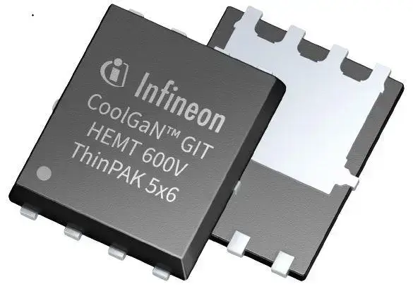
CoolGaN BDS: Bidirectional switch devices featuring an integrated common-drain dual-gate structure, capable of replacing traditional back-to-back switches while reducing chip area and parasitic components.
CoolGaN Drive: Integrated driver modules for half-bridge or single-switch configurations, reducing design complexity.
CoolGaN Smart: Smart devices incorporating current sensing and protection functions.
CoolGaN Control: System-in-package solutions supporting multi-topology integration.
| Technical Advantages
Body Diode-Free Design: GaN transistors have no physical body diode and feature zero reverse recovery charge (Qrr), making them suitable for hard-switching topologies (such as totem-pole PFC) while reducing switching losses and reliability risks.
Low Parasitic Parameters: Terminal capacitance and gate charge are significantly lower than silicon-based devices, supporting higher switching frequencies (up to MHz levels) and improving power density and efficiency.
Dynamic RDS(on) Optimization: Technologies, including buffer layer engineering and interface state control, are employed to mitigate dynamic on-resistance drift issues, enhancing device stability.
EPC (Efficient Power Conversion)
| Technology Positioning: Focuses on low-voltage and medium-voltage GaN devices, targeting high power density and high-efficiency power conversion applications such as data center power supplies, AI servers, humanoid robot motor drives, and satellite power systems.
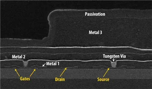
| Core Technology: Utilizes enhancement-mode Gallium Nitride on Silicon (eGaN®) FET technology, featuring low on-resistance (e.g., 0.84mΩ for EPC2366), low gate charge, and support for high-frequency switching operations, reducing conduction and switching losses. Emphasizes device reliability, having accumulated years of device reliability and durability data models to support large-scale procurement.
| Market Collaboration: It has established strategic partnerships with companies like Renesas, expanding market coverage and enhancing supply chain credibility through technology licensing and second-source arrangements.
Navitas Semiconductor
Navitas’s GaN business is characterized by technological leadership, high integration, and strong reliability, focusing on high-power, high-frequency application scenarios.
| GaNFast Technology: Integrates GaN power transistors with drive, control, and protection circuits on a single chip, achieving “digital in, power out.” It supports ultra-high switching frequencies (up to 2MHz), significantly improving power density and efficiency while reducing component count.
| High-Voltage Capability: Offers products with voltage ratings such as 650V and 100V, suitable for high-voltage DC conversion scenarios, including 800V architectures in data centers and high-voltage systems in electric vehicles.
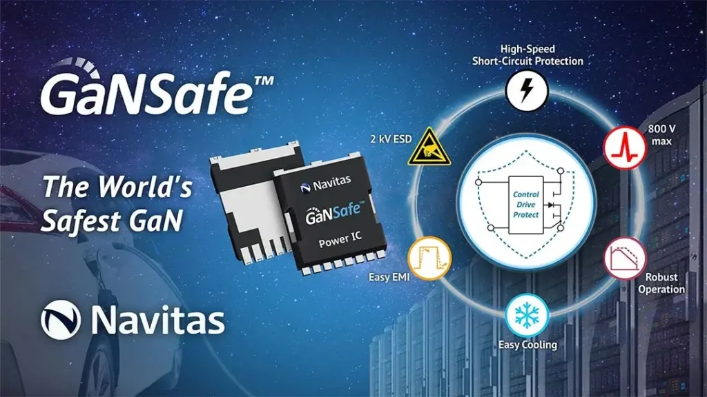
| Reliability Design: Integrates short-circuit protection (350ns delay), 2kV ESD protection, and programmable slew rate control. It is AEC-Q100/Q101 qualified for automotive applications, ensuring high reliability.
Product Series
GaNSafe™ IC: High-power GaN ICs suitable for on-board chargers and DC-DC converters. They feature bidirectional switching capability, supporting V2G (Vehicle-to-Grid) applications.
GaN FastFET: Discrete GaN transistors for high-frequency switching power supplies and motor drives. They offer low on-resistance (Rds(on)) and high current handling capability.
Full-Brick DC-DC Module: For example, the 10kW 800V-50V DC-DC platform utilizes a three-level half-bridge LLC resonant topology, achieving 98.5% peak efficiency. It is suitable for rack-level power conversion in data centers.
Texas Instruments
US company Texas Instruments leverages its deep expertise in analog chips to lower the application barrier through integrated solutions, charting a differentiated path for GaN deployment—focusing on the integrated design of medium- to high-voltage GaN power devices. Their core strategy involves integrating GaN chips with driver circuits, protection modules, and sensing units into a unified solution, offsetting dynamic effects at the system level and significantly reducing customer application and debugging complexity.
TI’s GaN products are primarily targeted at data center power supplies and industrial inverters. By enhancing system stability through integrated design and leveraging economies of scale in manufacturing, TI has achieved a gradual reduction in product costs, accelerating the penetration of GaN technology into mid-range industrial applications.
Innoscience
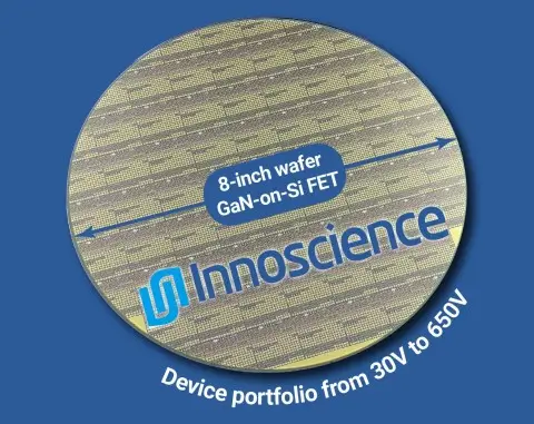
Pioneering the world’s first mass production of 8-inch GaN-on-Si wafers, utilizing a comprehensive IDM full-industry-chain model covering chip design, epitaxial growth, manufacturing, and testing to ensure full control over product quality and technology. Possesses full-voltage-spectrum GaN product technology, covering a voltage range from 15V to 1200V, including discrete devices, integrated circuits, and modules.
Product:
Represented by the “InnoGaN” series, featuring a P-GaN enhancement-mode device structure, offering advantages such as low on-resistance, high switching frequency, and low losses, suitable for high-frequency, high-power application scenarios.
Low-voltage products (e.g., 30V-40V) are suitable for consumer electronics, robotic joint drives, etc.; medium and high-voltage products (e.g., 650V-700V) are used in data center power supplies, new energy vehicle on-board chargers, photovoltaic inverters, and more.
Recommended In-depth Reading from AI Robots Eidos
GaN is critically important for robotics, especially humanoid robots. GaN technology provides technical support for the evolution of robots from “automation” to “embodied intelligence” by addressing core bottlenecks such as miniaturization, high efficiency, thermal management, and motion control.
If readers wish to gain a deeper understanding of GaN applications in the robotics field, please read this in-depth article on GaN technology.
ROHM
As one of the key Japanese GaN semiconductor companies, ROHM possesses significant advantages in high-voltage GaN technology.
| Product Series
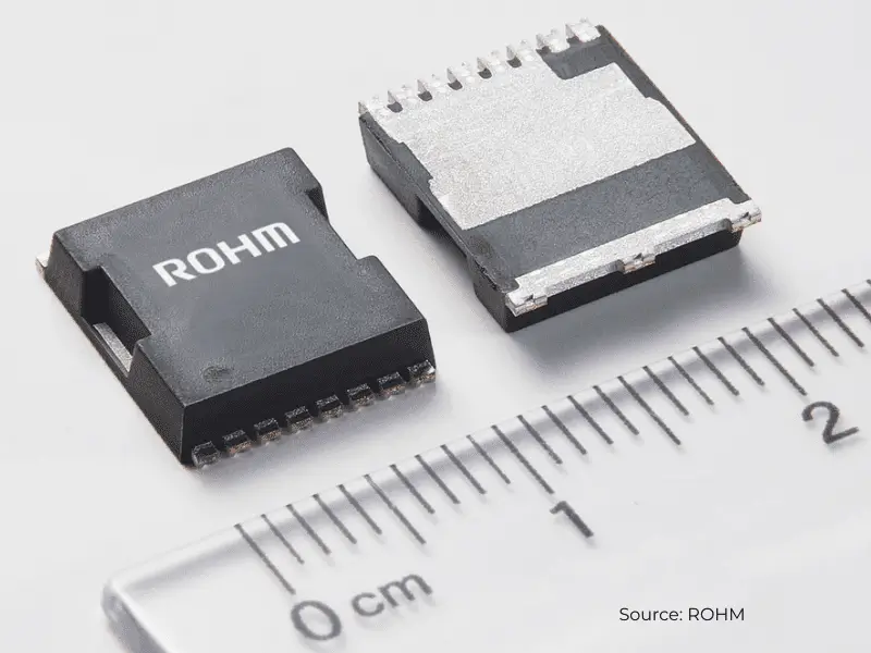
Discrete Devices: Includes 150V and 650V GaN HEMTs, such as the GNE10XXTB (150V) and GNP1070TC-Z (650V). These feature low on-resistance, high-speed switching characteristics, support high-frequency operation (switching frequencies exceeding 1MHz), and incorporate built-in ESD protection for enhanced reliability.
“nano cap” Series Power Stage ICs: These devices integrate GaN HEMTs, gate drivers, control ICs, and peripheral components into a single package. This simplifies design and reduces losses, making them suitable for applications such as AC-DC conversion and power factor correction.
| Business:
As an IDM (Integrated Device Manufacturer), ROHM produces GaN devices in its own factories while also collaborating with foundries like TSMC to leverage their process technology, increase production capacity, and ensure a stable supply.
Provides technical support through its FAE (Field Application Engineer) team, lowering the barrier to entry for customer application development and promoting the widespread adoption of GaN technology.
Onsemi
US semiconductor company onsemi focuses on a dual-technology roadmap with GaN-on-SiC and GaN-on-Si, primarily targeting high-end automotive and industrial applications. Their R&D efforts center around interface defect suppression and thermal stability optimization. By refining device structure design, they mitigate the impact of dynamic on-resistance drift and threshold voltage shift on automotive-grade applications. Their high-voltage GaN devices have passed stringent automotive certifications, making them suitable for on-board chargers (OBCs), automotive power modules, and similar applications.
STMicroelectronics (ST)
STMicroelectronics, an American company (Note: ST is actually a Franco-Italian multinational with significant operations in the US), centers its GaN business on “integration, miniaturization, and high efficiency.” Through technological innovation and a diverse product portfolio, it covers a wide range of fields from consumer electronics to industrial and automotive applications, driving the power electronics industry towards higher efficiency and smaller dimensions. ST has a foundry agreement with Innoscience to increase GaN device production capacity and reduce costs. Additionally, ST operates GaN production facilities in Tours, France, and Catania, Italy, supporting 8-inch wafer mass production to ensure supply chain stability.
List of Key Technical Features of GaN Semiconductor Companies and Manufacturers
| Company | Core Advantages & Characteristics |
| Innoscience | Vertically integrated (IDM) model, covering the full voltage spectrum from 15V to 1200V. 13,000 8-inch GaN-on-Si wafers are produced monthly. Strategic partnerships with NVIDIA and BYD. |
| Navitas Semiconductor | GaNSafe™ high-power GaN technology. Market leader in consumer electronics, fast charging. Secured orders from Enphase and NVIDIA data centers. Achieved 65% revenue growth in 2025. |
| EPC (Efficient Power Conversion) | Global leader in enhancement-mode GaN (eGaN®) technology. Absolute leader in low-voltage applications (<200V). Innovator in drones, robotics, and avionics. |
| Infineon | Strengthened position through the acquisition of GaN Systems. Leader in automotive-grade applications. Collaborating with NVIDIA to develop 800V solutions for data centers. |
| STMicroelectronics | Early entrant in the GaN business through the acquisition of Exagan. Formed a strategic 8-inch foundry partnership with Innoscience in 2025. Steadily increasing market share in automotive and industrial sectors. |
| Texas Instruments (TI) | Full value chain presence, from GaN epitaxy to modules. Rapidly increasing penetration in industrial and automotive markets. |
| Onsemi | Launched vertical GaN (vGaN) technology in 2025, achieving 3x smaller size than traditional lateral devices. Breakthrough in 1200V high-voltage applications. |
| ROHM | Strengths in high-voltage GaN technology. Developing automotive-grade solutions in partnership with Toshiba. Deep involvement in the industrial automation sector. |
The Technology Roadmap Debate among GaN Semiconductor Companies and Manufacturers: D-Mode Vs. E-Mode
As competition intensifies in the global GaN semiconductor market, technology roadmaps among GaN manufacturers are becoming increasingly divergent. Currently, mainstream GaN power device technologies fall into two major routes: D-Mode vs. E-Mode.
D-Mode (Depletion-mode)
| Characteristics: Normally-on devices requiring negative gate voltage drive. They offer excellent high-frequency performance and are suitable for high-voltage, high-power applications (e.g., charging stations, industrial power supplies). The industrial and automotive sectors tend to prefer D-Mode technology due to the superior reliability of products under high voltage and high temperature.
| Challenges: Require an external silicon MOSFET to achieve normally-off operation, leading to more complex drive circuit design, but excel in high-temperature reliability.
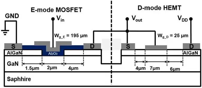
E-Mode (Enhancement-mode)
| Characteristics: Normally-off devices compatible with traditional silicon MOSFET drivers. They feature simpler circuit design and are well-suited for medium-to-low voltage scenarios like fast charging and servers. The consumer electronics industry favors E-Mode technology for its high integration and adaptability to existing systems.
| Challenges: Require special processes (e.g., p-GaN gate) to achieve normally-off operation, leading to relatively higher costs.
The choice between D-Mode and E-Mode often defines a company’s market strategy. Below, we analyze how different GaN semiconductor companies have aligned themselves with these technologies to serve specific industry needs.
GaN Semiconductor Companies and Manufacturers (E-Mode Technology Route)
| Manufacturer | Type |
|---|---|
| Navitas | Fabless |
| Innoscience | IDM |
| Infineon | IDM |
| EPC | Fabless |
| STMicroelectronics | IDM |
| ROHM | IDM |
| Onsemi | IDM |
GaN Semiconductor Companies and Manufacturers (D-Mode Technology Route)
| Manufacturer | Type |
| Texas Instruments ( | IDM |
| Transphorm | Fabless |
| GaNext | Fabless |
| VisIC | Fabless |
| Nexperia | IDM |
| CGD | Fabless |
| Toshiba | IDM |
Technological Development of GaN Semiconductor Companies and Manufacturers
Global GaN semiconductor companies and manufacturers are driving GaN devices towards higher voltage, higher power, and greater intelligence through technological iteration and innovation, meeting the demands of emerging applications such as robotics, AI data centers, and new energy vehicles.
| Enhanced High-Voltage and High-Power Capability: Developing higher voltage GaN devices (e.g., 1200V and above) to meet the needs of high-voltage power conversion in EVs, industrial motor drives, and grid applications. Optimizing device structures (e.g., vertical GaN technology, improved drift region design) to increase power density, achieve higher current output (e.g., single chip supporting over 170A), while reducing conduction and switching losses.
Insight from AI Eidos Robots about GaN Semiconductor Companies and Manufacturers
| Expansion of Bidirectional Switch Technology: Monolithically integrating bidirectional GaN switches (BDS) to replace traditional back-to-back switch configurations, simplifying circuit design, reducing parasitic components, and improving switching speed and efficiency. Expanding the application of bidirectional switches in areas like solar inverters, on-board chargers, AI server power supplies, and motor drives to enable bidirectional energy flow and more efficient power conversion.
| Innovations in Packaging and Integration Technologies: Adopting new packaging techniques (e.g., Intelligent Power Modules IPM, GaN power modules) to reduce stray and parasitic inductance, improve heat dissipation, and support higher power output (up to 70kW). Promoting vertical integration technologies like GaN-on-GaN and GaN-on-sapphire to optimize device performance and cost for different application scenarios.
| Integration of Control and Smart Functionalities: Integrating current sensing, temperature sensing, and fault detection functions into GaN devices for condition monitoring and self-protection, enhancing system reliability. Integrating with microcontrollers (MCUs) to support intelligent operation and predictive maintenance, meeting the smart power management needs of AI data centers and robotics.
| Breakthroughs in Materials and Substrate Technology: Exploring new materials like diamond substrates and engineered substrates to improve the thermal conductivity and breakdown voltage of GaN devices, addressing thermal management challenges in high-power applications. Optimizing sapphire substrate technology to reduce epitaxy costs and improve crystal quality, promoting the adoption of GaN devices in consumer electronics and low-power domains.
Insight from AI Robots Eidos about GaN Semiconductor Companies and Manufacturers
| The GaN industry is transitioning from the initial division of “design and manufacturing separation” to a new stage that emphasizes “system-level optimization requiring deep process coupling.” In the future, GaN semiconductor companies that possess their own fabs will establish a deeper moat in the high voltage and high power market.
| Future GaN Semiconductor Companies will essentially be advanced packaging solution providers. Those with a profound background in “third-generation semiconductor packaging” (such as low parasitic inductance packaging and dual-side heat dissipation packaging) will be able to enhance device performance further without altering the wafer design.
| The technical roadmap choices of GaN semiconductor companies essentially reflect their trade-offs between “performance density” and “economic density” in the target market. In the future, a successful GaN manufacturer must possess “multi-route management capabilities” or establish insurmountable patents and process barriers on a specific substrate route.
Image Credits: Infineon& Epc-co & Navitassemi & ROHM & Innoscience & Semanticscholar